How ai chips accelerate edge computing and what that means for devices and markets
Topics covered
- How AI chips are reshaping edge computing
- How the technology works
- Benefits and trade-offs
- Practical applications
- Market landscape
- Where things are headed
- Technical direction (engineer’s view)
- Implementation details (how it runs)
- Pros and cons (clear list)
- Deployment patterns and best practices
- Examples by sector
- Competition and consolidation
- Near-term outlook
How AI chips are reshaping edge computing
AI chips are purpose-built processors designed to run machine learning tasks far more efficiently than general-purpose CPUs. By moving inference — and even light retraining — to the point where data is generated, these chips slash latency, cut bandwidth use, and extend battery life.
Their secret sauce is a combination of massively parallel compute units, low‑precision arithmetic, and memory systems tuned for streaming neural workloads. The result: cameras, controllers, wearables and other edge devices can make split-second decisions without constant cloud round-trips, while keeping operational costs and power draw in check.
How the technology works
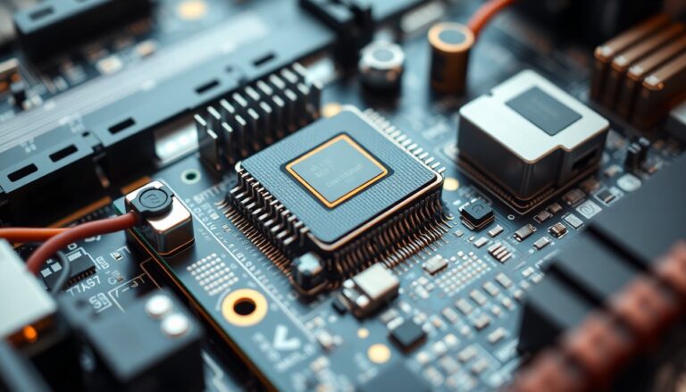
Modern edge accelerators lean into parallelism and energy thrift. Architects pack wide matrix multiply/accumulate units, systolic arrays or tensor cores into silicon and pair them with multi‑level on‑chip SRAM so weights and activations sit close to the compute.
To further shrink compute and memory footprints, engineers use quantization (often int8, increasingly int4) and sparsity-aware formats; pruning and compressed kernels are common. On the software side, model compilers and runtime engines perform operator fusion, layer reordering and other hardware-aware transforms that map neural networks into efficient tiled kernels. When hardware and software are designed together, throughput per watt improves dramatically.
Benefits and trade-offs
What you gain by moving AI to the edge:
– Much lower latency — decisions happen within milliseconds, not after a cloud round-trip.
– Far less upstream bandwidth — only the essential data or events are transmitted.
– Better privacy and compliance — sensitive raw data can be processed locally.
– Resilience to network outages — devices keep working when connectivity is intermittent.
– Lower ongoing cloud costs for high-volume workloads.
What you give up or must manage:
– Less raw compute than datacenter GPUs, which constrains model size and complexity.
– Fragmentation across vendors and runtimes, which raises portability and maintenance overhead.
– Need for model adaptation — quantization, pruning and operator adjustments can alter accuracy unless handled carefully.
– More complex lifecycle management: firmware, model updates and security patches must be pushed to many endpoints.
Practical applications
Edge AI chips are already powering a wide range of real-world systems:
– Cameras that run real-time object detection and only upload event clips.
– Industrial controllers that perform predictive maintenance at the line level.
– AR headsets and wearables that require frame‑tight inference without cloud lag.
– Drones and autonomous vehicles that fuse sensor data and act on it within milliseconds.
– Healthcare devices that monitor vitals and flag anomalies locally to preserve patient privacy.
Across these use cases, lightweight, quantized networks and hardware-aware model packing enable sustained operation on tight power budgets.
Market landscape
The ecosystem mixes big incumbents, mobile SoC vendors, specialist startups and cloud providers offering edge accelerators. Some chips optimize for throughput on batch workloads; others prioritize single‑query, ultra‑low latency. Adoption tends to follow where software ecosystems and toolchains are strongest — vendors that ship robust compilers, prebuilt model libraries and device management platforms win enterprise trust. Still, differing ISAs, runtime APIs and model formats keep fragmentation alive; standardization and better cross‑platform runtimes will be decisive for broader adoption.
Where things are headed
Expect continued convergence toward heterogeneous systems that pair general-purpose cores with domain-specific accelerators. Key trends likely to shape the next generation:
– Tighter hardware–software co‑design, with compilers that know the silicon intimately.
– Broader mixed‑precision support and native sparsity formats to squeeze more efficiency from models.
– Stronger on‑silicon security primitives and deterministic execution modes for real‑time workloads.
– Toolchains and standards that ease cross‑device deployment and lifecycle management.
Technical direction (engineer’s view)
Future edge processors look modular: tiled on‑chip memory, wide matrix multipliers, and deterministic dataflow primitives that minimize off‑chip transfers. Mapping compressed kernels and sparse operators onto these primitives reduces energy per inference and tightens latency bounds. Mixed‑precision and sparsity-aware execution yield substantial TOPS/W improvements, but designers must trade off flexibility for predictability when building systems for safety‑critical tasks.
Implementation details (how it runs)
Think of an AI chip as a power tool built for a narrow set of neural workloads. Systolic arrays or matrix‑vector units handle the heavy linear algebra, while on‑chip schedulers and local SRAM keep tensors within arm’s reach of the compute. Compilers translate high‑level models into tiled kernels tailored to the device: weights get quantized, some channels pruned, convolutions fused. Runtimes then schedule kernels to meet latency and power targets and expose primitives that help guarantee bounded execution — a must for control loops and safety systems.
Pros and cons (clear list)
Modern edge accelerators lean into parallelism and energy thrift. Architects pack wide matrix multiply/accumulate units, systolic arrays or tensor cores into silicon and pair them with multi‑level on‑chip SRAM so weights and activations sit close to the compute. To further shrink compute and memory footprints, engineers use quantization (often int8, increasingly int4) and sparsity-aware formats; pruning and compressed kernels are common. On the software side, model compilers and runtime engines perform operator fusion, layer reordering and other hardware-aware transforms that map neural networks into efficient tiled kernels. When hardware and software are designed together, throughput per watt improves dramatically.0
Modern edge accelerators lean into parallelism and energy thrift. Architects pack wide matrix multiply/accumulate units, systolic arrays or tensor cores into silicon and pair them with multi‑level on‑chip SRAM so weights and activations sit close to the compute. To further shrink compute and memory footprints, engineers use quantization (often int8, increasingly int4) and sparsity-aware formats; pruning and compressed kernels are common. On the software side, model compilers and runtime engines perform operator fusion, layer reordering and other hardware-aware transforms that map neural networks into efficient tiled kernels. When hardware and software are designed together, throughput per watt improves dramatically.1
Deployment patterns and best practices
Modern edge accelerators lean into parallelism and energy thrift. Architects pack wide matrix multiply/accumulate units, systolic arrays or tensor cores into silicon and pair them with multi‑level on‑chip SRAM so weights and activations sit close to the compute. To further shrink compute and memory footprints, engineers use quantization (often int8, increasingly int4) and sparsity-aware formats; pruning and compressed kernels are common. On the software side, model compilers and runtime engines perform operator fusion, layer reordering and other hardware-aware transforms that map neural networks into efficient tiled kernels. When hardware and software are designed together, throughput per watt improves dramatically.2
Examples by sector
- – Consumer: NPUs on phones power always‑on sensors, local voice assistants and on-device photography enhancements.
- Industrial: Rugged accelerators run visual inspection and anomaly detection right on the line, cutting downtime.
- Automotive: Low‑latency perception stacks for driver monitoring and ADAS use deterministic inference pipelines.
- Healthcare: Point‑of‑care modules perform preliminary diagnostics without sending protected data to the cloud.
- Smart cities: Edge analytics in cameras and sensors filter and act on events quickly, reducing central processing loads.
Competition and consolidation
Modern edge accelerators lean into parallelism and energy thrift. Architects pack wide matrix multiply/accumulate units, systolic arrays or tensor cores into silicon and pair them with multi‑level on‑chip SRAM so weights and activations sit close to the compute. To further shrink compute and memory footprints, engineers use quantization (often int8, increasingly int4) and sparsity-aware formats; pruning and compressed kernels are common. On the software side, model compilers and runtime engines perform operator fusion, layer reordering and other hardware-aware transforms that map neural networks into efficient tiled kernels. When hardware and software are designed together, throughput per watt improves dramatically.3
Near-term outlook
Modern edge accelerators lean into parallelism and energy thrift. Architects pack wide matrix multiply/accumulate units, systolic arrays or tensor cores into silicon and pair them with multi‑level on‑chip SRAM so weights and activations sit close to the compute. To further shrink compute and memory footprints, engineers use quantization (often int8, increasingly int4) and sparsity-aware formats; pruning and compressed kernels are common. On the software side, model compilers and runtime engines perform operator fusion, layer reordering and other hardware-aware transforms that map neural networks into efficient tiled kernels. When hardware and software are designed together, throughput per watt improves dramatically.4